For anyone in automotive electronics repair, especially when working with systems like key fob programming represented by websites like keyfobprog.com, understanding schematic diagrams is absolutely crucial. At the heart of diagnosing and fixing electrical issues lies the ability to interpret what we can call the component location diagram – though more formally known as a schematic diagram. This diagram isn’t a map of physical locations in the car, but rather a blueprint that shows how electronic components are connected and function together within a system.
Decoding Schematic Symbols: The Language of Electronics
Schematic diagrams use standardized symbols to represent different electronic components. Think of these symbols as a universal language for electronics. Two primary standards govern these symbols globally:
IEC 60617: Developed by the International Electrotechnical Commission (IEC), this standard, rooted in the older British Standard (BS 3939), is a comprehensive database with over 1750 schematic symbols. It is widely adopted internationally.
ANSI standard Y32: The American National Standards Institute (ANSI) standard provides another set of symbols, initially tailored for aircraft applications. Over time, revisions have aligned it closely with the IEC standard, ensuring greater consistency across different regions and industries.
Understanding these standards and their associated symbols is the first step in effectively using a component location diagram.
Common Schematic Symbols in Automotive Circuits
Automotive circuits, like any electronic system, rely on a set of standardized symbols within their component location diagrams. These diagrams illustrate the connections between various electronic components using these symbols.
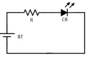
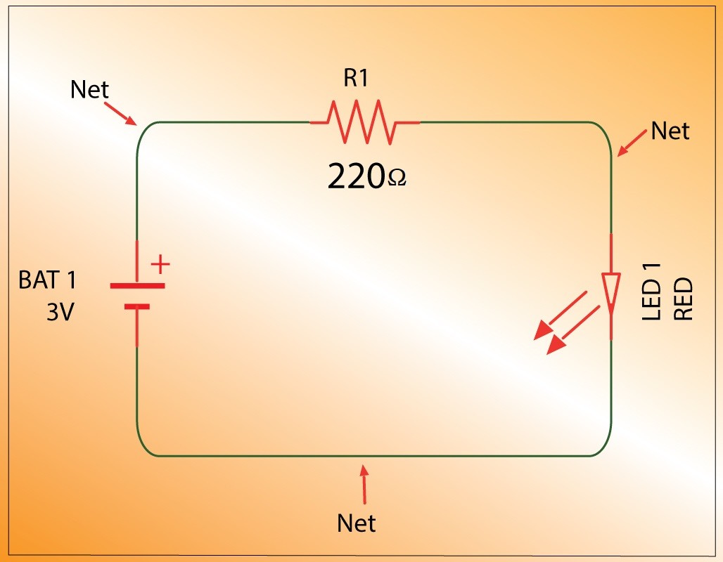
Fig. a: Basic schematic diagram
Consider a simple circuit in a car, perhaps related to the remote locking system. A simplified component location diagram might show components like a battery, a resistor, and an LED (representing an indicator light). These are connected by lines representing wires or traces. Each component is depicted by its unique symbol, and each symbol carries attributes.
For instance, a resistor symbol in a component location diagram will not only represent a resistor but can also be associated with attributes like its reference designator (e.g., R1), resistance value, size, tolerance, power rating, and even its physical footprint. Similarly, symbols for batteries, LEDs, sensors, and integrated circuits in automotive diagrams will have their own specific attributes.
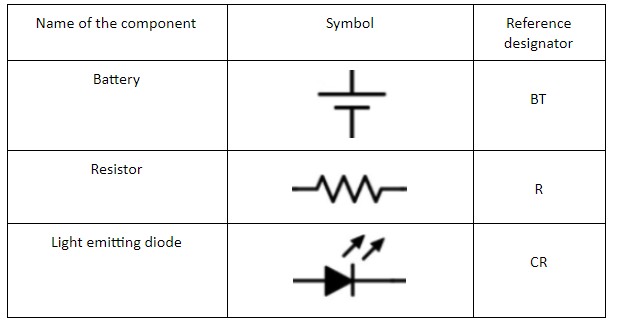
The table below shows some common schematic symbols and their reference designators you’ll frequently encounter in automotive component location diagrams. These designators (like BT for battery, R for resistor, LED for light-emitting diode, U for ICs, etc.) are crucial for identifying components within the diagram and on the actual circuit board.
Schematic symbols
By learning these symbols and their reference designators, technicians can effectively interpret any component location diagram and use it as a guide for diagnostics and repair.
Values and Attributes: Essential Details in the Diagram
While symbols and reference designators help identify components, a useful component location diagram goes further by providing crucial information about component specifications. Looking back at our basic circuit example (Fig. a), the diagram shows a battery connected to an LED through a resistor. However, without additional details, we don’t know the resistor’s resistance value or the battery’s voltage.
A comprehensive component location diagram includes these vital attributes. Resistors are labeled with their resistance in ohms (Ω), capacitors with capacitance in farads (F), inductors with inductance in henrys (H), and batteries with their potential difference (voltage) in volts (V).
Beyond these basic values, automotive component location diagrams often include other critical attributes:
- Symbol Shape and Pins: The visual representation of the component and its connection points.
- Values: Resistance, capacitance, inductance, voltage, etc.
- Reference Designators: U1, R1, C1, etc., for unique identification.
- Maximum Operating Conditions: Voltage or current limits, power ratings.
- Tolerances: Precision levels, e.g., ±1%, ±5% for resistors.
- Manufacturer Part Number (MPN): Specific part identification for replacement.
- Component Footprints: Physical size and package style (e.g., 0805 resistor, SOIC8 IC).
These attributes are essential for selecting the correct replacement parts and understanding the circuit’s operational parameters.
SI Units: Standardizing Values in Schematics
To manage the vast range of values encountered in electronics, from tiny currents to large voltages, component location diagrams utilize the International System of Units (SI). This system employs prefixes to represent magnitudes, avoiding long strings of zeros.
The table below lists SI prefixes commonly used in schematic diagrams:
| Prefix | Symbol | Value | Powers of 10 |
|---|---|---|---|
| tera | T | 1000000000000 | 1012 |
| giga | G | 1000000000 | 109 |
| mega | M | 1000000 | 106 |
| kilo | k | 1000 | 103 |
| milli | m | 0.001 | 10-3 |
| micro | µ | 0.000001 | 10-6 |
| nano | n | 0.000000001 | 10-9 |
| pico | p | 0.000000000001 | 10-12 |


Understanding these prefixes is essential for correctly interpreting the values indicated in a component location diagram. For example, reading “10kΩ” for a resistor immediately translates to 10,000 ohms.
Schematic Diagrams vs. Wiring Diagrams: Understanding the Difference
It’s important to distinguish a component location diagram (schematic diagram) from a wiring diagram. While both represent electrical circuits, they serve different purposes and present information in different ways.
In a schematic diagram (our component location diagram focus), lines represent electrical connections, and symbols represent components. It focuses on the functionality and connectivity of the circuit.
An example of a schematic diagram
A schematic diagram doesn’t depict the physical arrangement or location of components. It’s a logical representation, not a physical one.
On the other hand, a wiring diagram is a pictorial representation of an electrical circuit. It uses simplified shapes for components and emphasizes the physical connections and locations of components and wires. Wiring diagrams are crucial for assembly and physical wiring, showing the relative positions and arrangements of devices.
An example of a wiring diagram
For automotive electronics repair, especially at a component level (as often needed in key fob programming and related work), the component location diagram (schematic diagram) is generally more valuable for understanding circuit operation and troubleshooting. Wiring diagrams are more helpful for tasks like installing accessories or tracing physical wire runs.
Reading a PCB Schematic: Step-by-Step Interpretation
To effectively utilize a PCB schematic, which we’re considering as our component location diagram, you need to understand how components are connected and the information it conveys. A schematic provides a wealth of data about the circuit:
- Components Used: Identified by symbols and reference designators.
- Electrical Connections: Shown by lines (nets) connecting component pins.
- Operating Conditions: Voltage levels, current paths, tolerance values, and component ratings.
- Special Instructions: Information on impedance control, differential pairs, placement requirements for decoupling capacitors, crystals, and other sensitive components.
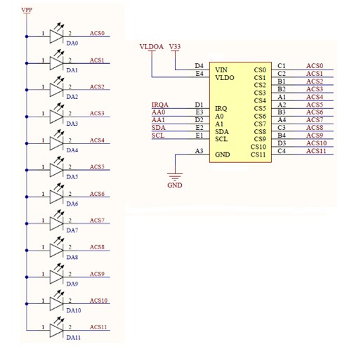
- Block Diagrams: For complex schematics, sections may be represented as functional blocks.
- Revision History: Indicates diagram updates and changes (if applicable).
Schematic Nets: Defining Connections
In a component location diagram, “nets” are the lines that illustrate electrical connections between components. A net represents a conductive path connecting component pins.
Nets in a basic schematic diagram
To learn more about ensuring error-free designs, resources on schematic and netlist checks are valuable.
Junctions and Nodes: Points of Connection
“Junctions” are points where two or more wires intersect and are electrically connected. In a component location diagram, these junctions are marked with a small dot or “node.”
Representation of nodes in a schematic diagram
Nodes clearly indicate connections. Crucially, if wires cross without a node, it means they are not electrically connected; they are simply passing over each other.
Naming Schematic Nets: Enhancing Clarity
To improve readability, especially in complex component location diagrams, nets are often labeled with names instead of being drawn as continuous lines across the diagram. Nets with the same name are assumed to be connected, even if no line physically joins them on the drawing.
Schematic with labeled nets
Net names are essential for tracing signals and understanding circuit flow in larger, more intricate schematics.
Schematic Diagram vs. PCB Layout: Logical vs. Physical Representation
The schematic diagram, our component location diagram, defines the logical connections between components, whether for a rigid PCB or a flex board. It shows how components are electrically linked, regardless of their physical positions. A schematic essentially contains a “netlist,” a data file detailing all the connections.
An example of a PCB schematic diagram
In contrast, the PCB layout shows the physical locations of components on the PCB and the physical traces (copper wires) connecting them. It’s a representation of the actual circuit board’s physical construction.
An example of PCB layout
Understanding this distinction is key. The component location diagram (schematic) is for understanding circuit function; the PCB layout is for physical realization and manufacturing.
PCB DESIGN TOOL
BOM Checker
TRY TOOL
Creating a Schematic Diagram: Building the Blueprint
Creating a component location diagram usually involves using PCB CAD (Computer-Aided Design) tools. For complex designs, hierarchical schematics are often used, where functional blocks are interconnected across multiple sheets, making the diagram more manageable.
The process of schematic creation generally includes:
Symbol Generation: Creating or selecting symbols for components. This involves defining the symbol’s graphical representation, adding pins, assigning pin numbers, and defining attributes and footprints. Many CAD tools have pre-built symbol libraries. Resources like creating schematic symbols in KiCad offer guidance.
Component Symbol Placement: Placing the selected symbols onto the schematic workspace within the CAD software.
Guidance on component placement is helpful for efficient schematic design.
Pin Numbering: Ensuring correct pin assignments to match component functionality and physical connections.
Symbol Attributes: Adding relevant data to each symbol, such as category, value, manufacturer, part number, and supplier information. Unique reference designators are crucial for each component for easy identification.
PCB DESIGN TOOL
Better DFM
TRY TOOL
Rules for Drawing Schematic Diagrams: Best Practices
Adhering to best practices when drawing component location diagrams ensures clarity and accuracy. Key rules include:
- Connection Representation: Lines represent connections. Intersecting lines are only connected if a node is present.
- Node Connections: Ideally, limit nodes to a maximum of three connecting lines for clarity.
- Net Naming: For complex circuits, use net names to indicate connections, improving readability.
- Text Orientation: Keep pin numbers, polarities, values, and net names horizontal for easy reading.
- Input/Output Placement: Generally, place inputs on the left and outputs on the right to indicate signal flow.
- Functional Blocks: Organize the schematic into functional blocks for logical organization.
- Pin Number Placement: Always place pin numbers outside the component symbol graphic.
- Sheet Connection Symbols: Place sheet connection symbols (for multi-sheet schematics) at the edges of the page.
- Title Block: Include a title block in the lower right corner of the first sheet with:
- Title
- Part number
- Revision (if any)
By following these rules, designers and technicians can create and interpret component location diagrams effectively, leading to successful PCB design and efficient troubleshooting in automotive electronics and areas like key fob programming. Understanding the component location diagram is indeed fundamental for anyone working with electronic circuits.
[